
🛠️ Ready for the Bench?
Before diving into the hardware assembly, we highly recommend verifying your signals in a risk-free environment first. If you haven’t already, take a look at our guide on how to simulate the ESP32 galvanic isolation circuit in Falstad to watch the real-time back-EMF suppression waveforms in action.
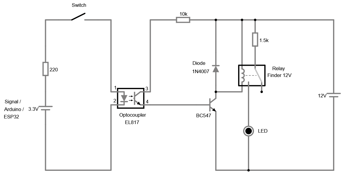
Figure 1: The updated circuit simulation layout.
💡 Pro Hardware Safety Practice: Notice the updated configuration of our test circuit. Connecting current-limiting resistors directly to the primary power source nodes is an excellent fail-safe bench habit. By anchoring the resistors directly at the source, any trace line or component pulled downstream from that node is automatically limited to a weak, safe current window. This prevents catastrophic component damage if you make an accidental wiring error, compared to pulling a raw un-resisted wire path directly from a raw voltage supply rail.
Look closely at the layout topology: the control switch pulls its trigger signal directly from after the current-limiting resistor rather than tying straight onto the raw power line. The second resistor actively throttles the path down to the optocoupler’s sensitive LED input, while the third resistor handles safety overhead down the line toward the transistor driver and relay loop.
Having mapped out and verified our protection circuit in simulation, we can now transition the design onto a physical breadboard. This hands-on project acts as a hardware defensive shield, converting a weak, sensitive 3.3V control pulse into a robust switching channel without exposing your microcontroller to catastrophic noise or spike feedback loop damage.
The Bench Architecture: Physics Behind the Transistor Driver
A typical logic chip pin cannot provide enough electrical output to pull down a large mechanical relay coil magnet. For example, a 12V Finder Relay (40.52.9.012.0000 Power Relay) coil draws around 54mA of continuous current to close its internal armature switches. The internal phototransistor inside an optocoupler safe-zone boundary is too delicate to sustain this high electrical current stream directly.
We use an NPN transistor(BC547 can handle a 100mA Continuous Collector current (IC)) to handle this heavy lifting. By injecting a tiny signal current from the optocoupler’s active side into the base pin of our transistor, we force it into saturation (full switch-on mode). The transistor instantly behaves like an automated low-resistance valve, grounding out the relay coil circuit path to source the current required from your high-voltage loop without breaking a sweat.
Step-by-Step Bench Prototyping Assembly Guide
Follow these construction steps sequentially to establish independent power rails and avoid cross-contaminating your isolation domains.
Step 1: Wire Up Your Control Input Power Loop
- Prepare your control voltage input source. You can use two 1.5V batteries connected in series, a dedicated workbench power supply tracking tool, or the direct 3.3V logic output pin from your active ESP32 board.
- SETTING UP THE SIGNAL ZONE: Connect this low-voltage supply positive wire strictly to the top power rail on the LEFT half of your breadboard. Ground out its negative connection pin directly to the bottom lower rail on the LEFT half.
- OPTOCOUPLER ORIENTATION: Insert your EL817 optocoupler chip firmly across the center horizontal plastic dividing channel split of your breadboard around column 30. This places your signal inputs (Anode Pin 1 / Cathode Pin 2) on the TOP half of the board, and the phototransistor outputs (Collector Pin 4 / Emitter Pin 3) on the BOTTOM half.
- Following our high-safety resistor routing rule, run a jumper wire directly from your 3.3V power source node straight into one terminal of your 220 Ohm current-limiting resistor.
- Route the output from that resistor through your push-button switch or ESP32 control wire, and land it directly on Pin 1 (Anode) on the top half of the optocoupler chip body. By keeping the resistor first, the switch handles only weak, safe current.
- Complete the input loop by running a wire from Pin 2 (Cathode) on the top half of the optocoupler directly to your LEFT-side bottom ground rail.
Step 2: Initialize Your Isolated High-Power Rails
- Set up your secondary power loop network. For this practical test layout, we will deploy the high-efficiency step-up Automatic Buck-Boost Converter Module configuration analyzed in our earlier hardware post.
- Feed any entry-level voltage between 5.5-30V DC input adapter signal directly into the buck converter module’s incoming voltage terminals.
- Hook up a digital multimeter tool across the buck converter output terminal lugs, and rotate its brass potentiometer screw CV adjustment head until the output voltage matches exactly 12V DC.
- Connect the new isolated 12V positive wire strictly to the top power rail on the RIGHT half of your breadboard.
- Connect its matching negative ground wire straight to the bottom lower rail on the RIGHT half.
- REMINDER: Keep the left-side (3.3V) and right-side (12V) ground paths completely separate to preserve your galvanic isolation. Do not bridge the power lines across the middle.
Step 3: Build the Transistor Driver Configuration
- Insert your BC547 NPN transistor firmly into an unlinked grid cluster on the BOTTOM-RIGHT half of your breadboard.
- TRANSISTOR ORIENTATION: Position the transistor so that its Collector pin sits on the right side to receive the upcoming load connections. The Base pin sits in the middle, and the Emitter pin maps toward the ground rail path.
- Run a wire track from Pin 4 (Emitter) of your optocoupler—located on the bottom half of the board—straight to your BC547 Base.
- Connect Pin 3 (Collector) of your optocoupler through your 10k Ohm base resistor. The 10k resistor’s other end goes to the +12V.
- Connect the Emitter pin of your BC547 transistor directly down onto your isolated RIGHT-side bottom ground rail to anchor the circuit.
Step 4: Connect the Finder Relay & Back-EMF Protection
- Mount your 12V Finder Relay (or equivalent voltage model variant) onto your breadboard footprint grid. Always verify the manufacturer pinout map to confirm which two pins connect directly to the inner activation coil loop.
- Wire one end of the relay coil connection terminal straight to the isolated 12V DC positive power bus line. Connect the remaining coil terminal terminal wire right down onto the collector pin of your NPN transistor.
- Insert your 1N4007 Diode parallel across the relay coil terminals. The silver stripe (cathode ring) must point towards the positive 12V rail. This configuration clamps sudden back-EMF voltage spikes when the relay turns off, routing current away from the transistor.
Step 5: Add the Status LED Output Indicator
- Rather than switching a dangerous 220V appliance directly during this initial bench test, we will use a low-power status LED indicator to confirm when the relay contact clicks.
- Identify the Normally Open (NO) switch contact terminal pins and the central Common (COM) pin leg positions on your 12V Finder relay case.
- Following our high-safety resistor routing rule, connect a 1.5k Ohm resistor directly from your 12V DC positive rail on the right side of the board to protect your diagnostic LED (12V / 1500Ω = 8mA, which is perfect and safe for this quick test).
- Route the output from this 1.5k Ohm resistor straight into the COM pin of the relay.
- Run a wire track directly from the relay’s NO contact pin to the long leg (Anode +) of your diagnostic LED.
- Complete the output loop by connecting the short leg (Cathode -) of the LED straight to the RIGHT-side bottom ground rail (12VDC ground).
🛠️ Bench Diagnostic & Troubleshooting Guide
A reliable digital multimeter is necessary in any case for troubleshooting, even though the circuit footprint remains fundamentally simple. To verify that your high-power output configuration is working properly without involving the logic side, follow this diagnostic routine:
- Test the High Power Domain: Take a small jumper wire and deliberately short-circuit the lower output pins of the optocoupler together (Pin 3 and Pin 4).
- What to Look For: This manually forces the 12V rail current straight into the base of the BC547 NPN transistor. If the output stage is wired correctly, the transistor will instantly fully ground out, energizing the Finder relay coil. You should hear a clear mechanical click and see the red status LED light up instantly.
- If the test fails, use your multimeter to verify a clean 12V rail output on the right side and cross-reference your BC547 pin orientation layout.
Engineering Advice: Switching DC vs. AC Field Loads
While this bench test layout focuses on a 12VDC loop, real-world relays frequently bridge into high-power alternating current (AC) machinery. Understanding the distinct stress elements of DC and AC loads on mechanical contacts is vital for your circuit’s operational lifespan.
1. Switching DC Loads (High Arc Risk)
Direct current maintains a continuous voltage level without ever dropping to a zero baseline. When physical relay contacts separate under heavy DC load conditions, a continuous electric spark (arc) forms across the widening physical gap. This high-temperature arc slowly melts, pits, and degrades the contacts over time.
- Safety Rating: A relay rated to switch 10A at 250VAC can typically only handle 10A up to 30VDC before arc degradation risks lock the contacts permanently shut.
- Suppression Fix: Always use a flyback diode (like a 1N4007) across inductive DC loads to clamp high-voltage spikes, or deploy an RC Snubber circuit across the contacts.
2. Switching AC Loads (Zero-Crossing Advantage)
Alternating current oscillates back and forth continuously, dropping down to pass through 0V exactly twice during every complete frequency cycle. This continuous zero-crossing behavior naturally extinguishes forming contact arc points quickly.
- Safety Rating: Relays can comfortably manage significantly higher voltage potentials (250VAC+) without premature contact erosion.
- Suppression Fix: Inductive AC field devices (motors, transformers) throw highly destructive phase-shifted noise vectors. Always wire a dedicated Metal Oxide Varistor (MOV) or AC-rated RC snubber network in parallel across the switching relay contacts to protect the system.
📷 Bench Lab Verification Verification
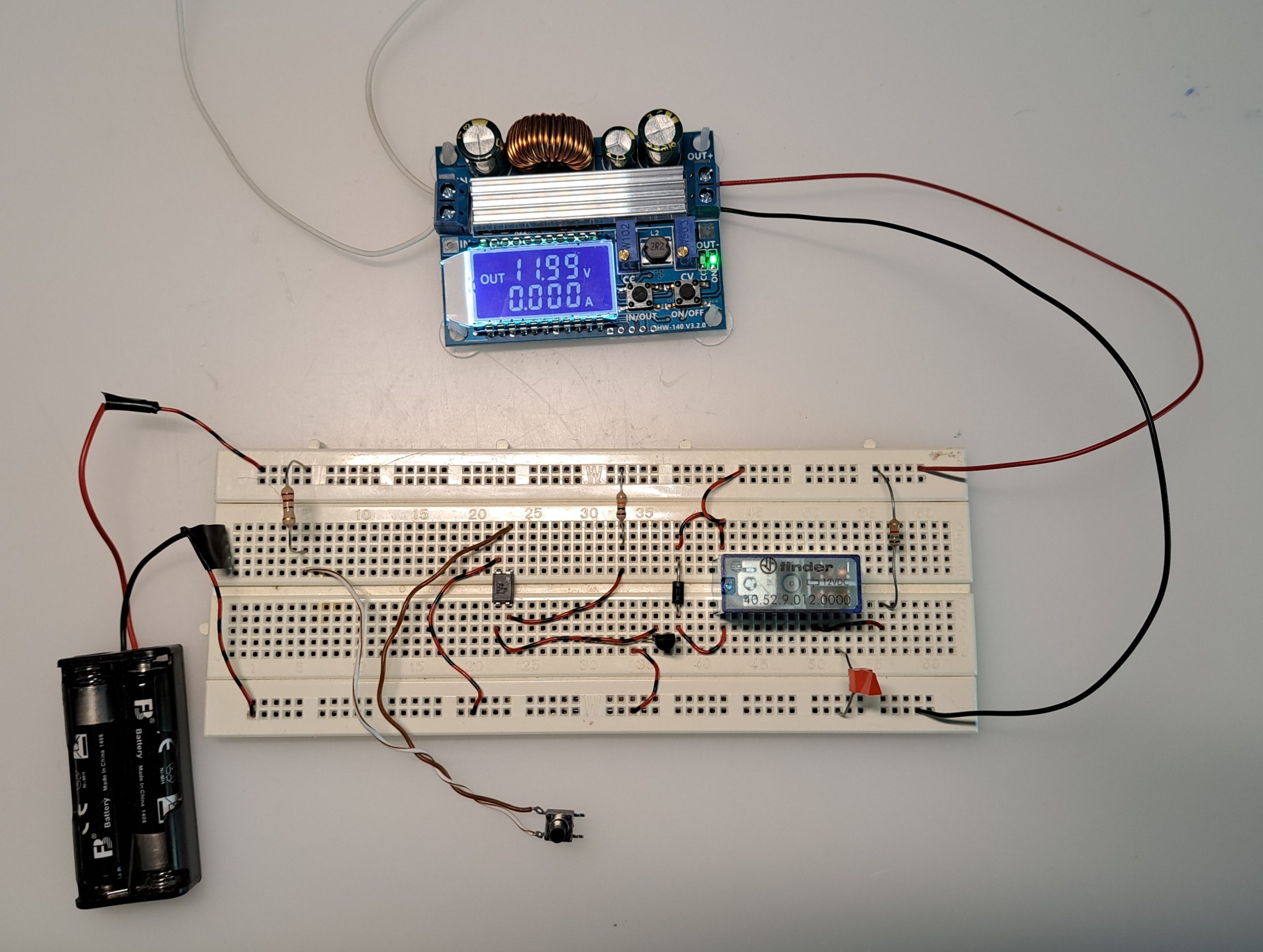
Figure 2: The final physical circuit assembly in its baseline idle (OFF) state. The buck-boost module reads a stable 11.99V output routed strictly to the isolated right-hand distribution power rail.
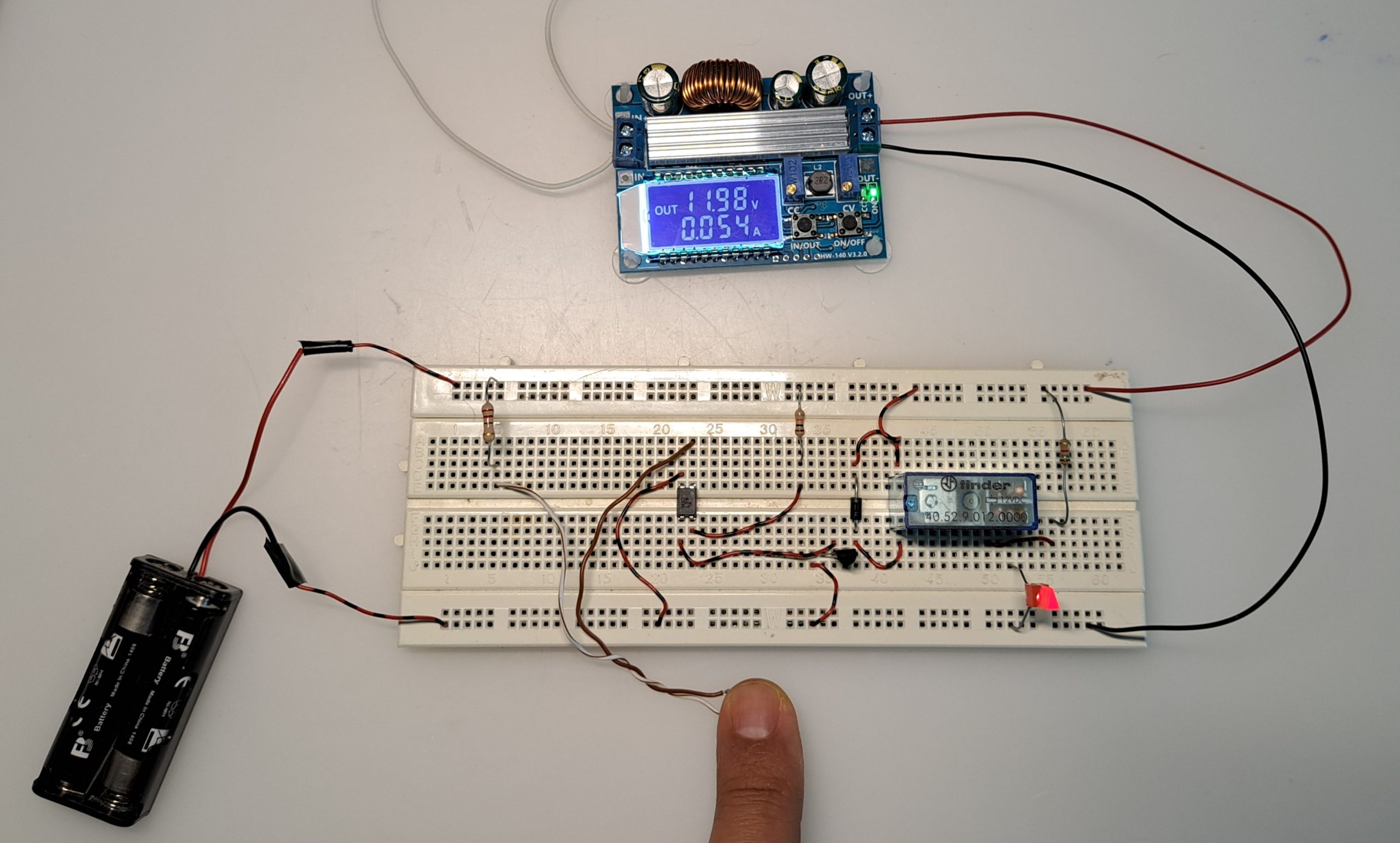
Figure 3: Active system test state with the tactile switch pressed. The EL817 isolates the trigger, the BC547 drives the 12V Finder relay coil, and the red diagnostic indicator LED glows bright to confirm output closure.