
Industrial environments expose microcontrollers to destructive electrical hazards. High-voltage spikes, inductive back-EMF, and ground loops can instantly fry a delicate 3.3V ESP32. To build an uncompromised protection shield, you must separate your logic from heavy field loads using a three-tier defensive topology.
The 3-Tier Defensive Architecture
True galvanic isolation completely breaks the copper path between your control logic and the high-power machine environment:
- Tier 1: Optocoupler (Optical Isolation) – Converts the ESP32 electrical signal into light via an internal LED. An internal phototransistor detects this light to switch the secondary side without physical electrical contact.
- Tier 2: Transistor Driver (Current Amplification) – Internal phototransistors cannot handle the high current demands of physical relay coils. An external NPN transistor acts as a power valve to safely ground the coil.
- Tier 3: Mechanical Relay (Physical Load Isolation) – Physically moves an armature to switch the heavy machine loads independent of your system voltages.
Engineering Calculation: 3.3V ESP32 LED Resistor
To safely drive the internal LED of a standard PC817 optocoupler directly from an ESP32 GPIO pin without burning out the output pin or the LED, we must calculate the exact current-limiting resistor value.
The Parameters:
- ESP32 GPIO Output Voltage (Vcc): 3.3V
- PC817 LED Forward Voltage Drop (Vf): 1.2V (typical)
- Target Continuous Operating Current (If): 10mA (0.01A)
The Formula:
R = (3.3V – 1.2V) / 0.01A
R = 2.1V / 0.01A = 210 Ohms
For reliable real-world deployment, use a standard, easily accessible 220 Ohm resistor.
Step-by-Step Falstad Simulation Guide
Follow these structured configuration steps to construct, test, and analyze your isolation circuit directly inside your web browser window.
Step 1: Workspace Setup & Input Stage
- Visit the browser app address: falstad.com.
- Navigate to the upper-left navigation bar and select File > New Blank Circuit to wipe the canvas clean.
- Go to the main dropdown menu and choose Draw > Active Building Blocks > Add
Optocoupler. Click and drag your mouse cursor onto the empty workspace grid to place your
component. Hit ESC on your keyboard to drop the active placement tool.
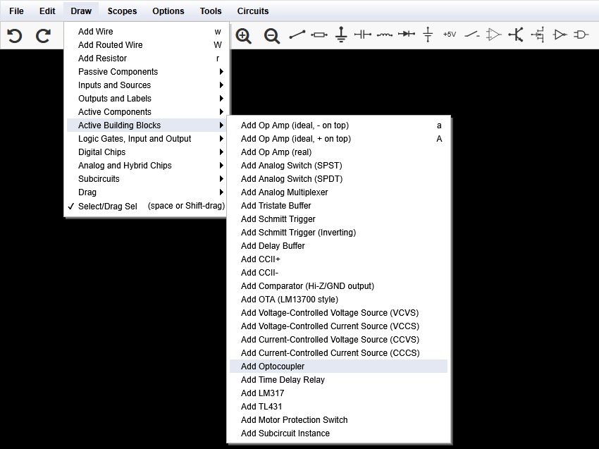
Figure 1: Placing the Optocoupler to the Canvas.
- Locate the visual selection toolbar positioned near the top of the interface screen. Click to insert a
DC Power Source, a Switch, and a standard Resistor
into your canvas layout.
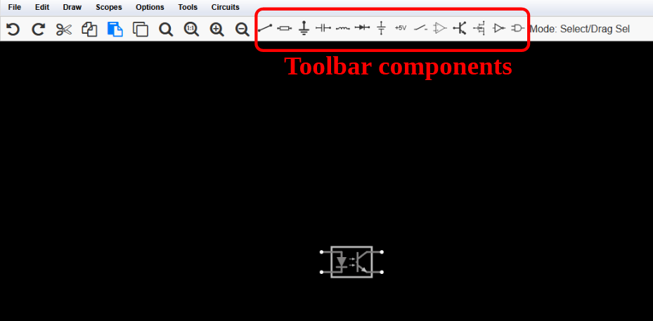
Figure 2: The toolbar and the Optocoupler placed to the Canvas.
- Double-click over your new DC power source component to open its options panel, and modify its value setting to exactly 3.3V to mirror the precise hardware voltage parameters of an ESP32 GPIO pin.
- Double-click directly over your newly placed input resistor to open its settings window, and reconfigure its electrical resistance value parameter to read 220 Ohms based entirely on our engineering calculations.
- Press the W key on your keyboard to instantly engage the dedicated path wiring tool.
Carefully draw lines to snap the glowing white connection dots together, creating a loop between the
power source, the switch, the resistor, and the input terminals on the left side of your optocoupler.
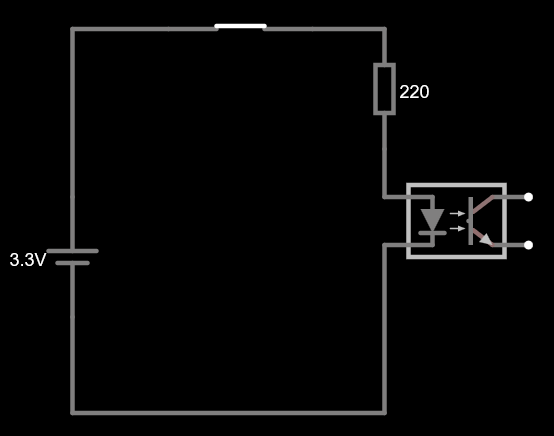
Figure 3: The circuit will look like this now.
Step 2: Constructing the High-Power Output Loop
- Select and place an NPN Transistor and another standard Resistor on your canvas grid, positioned directly near the right output side of your optocoupler.
- Double-click this base resistor to open its properties, and modify its value configuration parameter to 10k Ohms to balance the driver activation current. Wire it between your optocoupler collector supply line and the physical base pin of your NPN transistor.
- Open the selection menu bar and click Draw > Passive Components > Add Relay (or press the keyboard shortcut R). Position the relay symbol directly above your transistor node.
- Select a standard Diode from the interface toolbar. Wire it in a reverse-biased (parallel but upside-down) direction across the relay coil terminals. This acts as a freewheeling/flyback protection diode to redirect destructive inductive back-EMF voltage spikes away from your transistor when the relay coil turns off.
- Place a second completely independent DC Power Source onto your right-side workspace area. Double-click it and update its voltage parameter string to 24V to mirror a typical industrial control power system.
- Navigate to the top dropdown menu options and select Draw > Outputs and Labels > Add
Lamp to represent your isolated machine load field device. Engage your wire path tool
(W) and connect all remaining open pins to finish the circuit footprint.
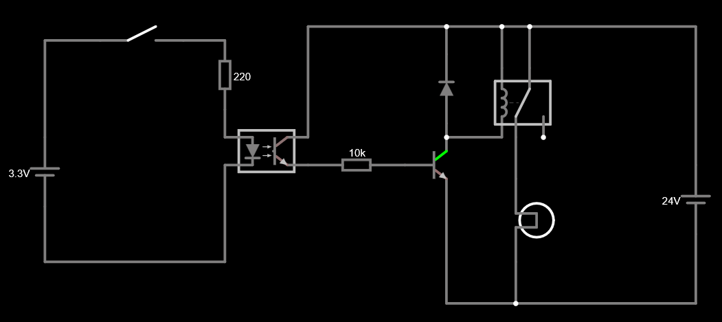
Figure 3: The final ready circuit.
Step 3: Real-Time Waveform Scope Diagnostics
- Right-click directly over your Lamp component and select View in a New Scope. A graphical tracing window will open at the bottom of the canvas area.
- Right-click inside this fresh scope box, open Properties, and lower the Horizontal Scale parameter to 200 ms/div to slow down visual sweep progression for accurate monitoring.
- Navigate to the speed configuration sliders on the top right edge of your browser screen. Drag the Simulation Speed cursor to its maximum limit.
- Click the global Run/STOP button to begin the live execution.
- Click your canvas switch to cycle it ON and OFF. The diagnostic scope window will visualize the
immediate peak current rising instantly when the switch closes, stabilizing smoothly as the high-voltage
lamp lights up.
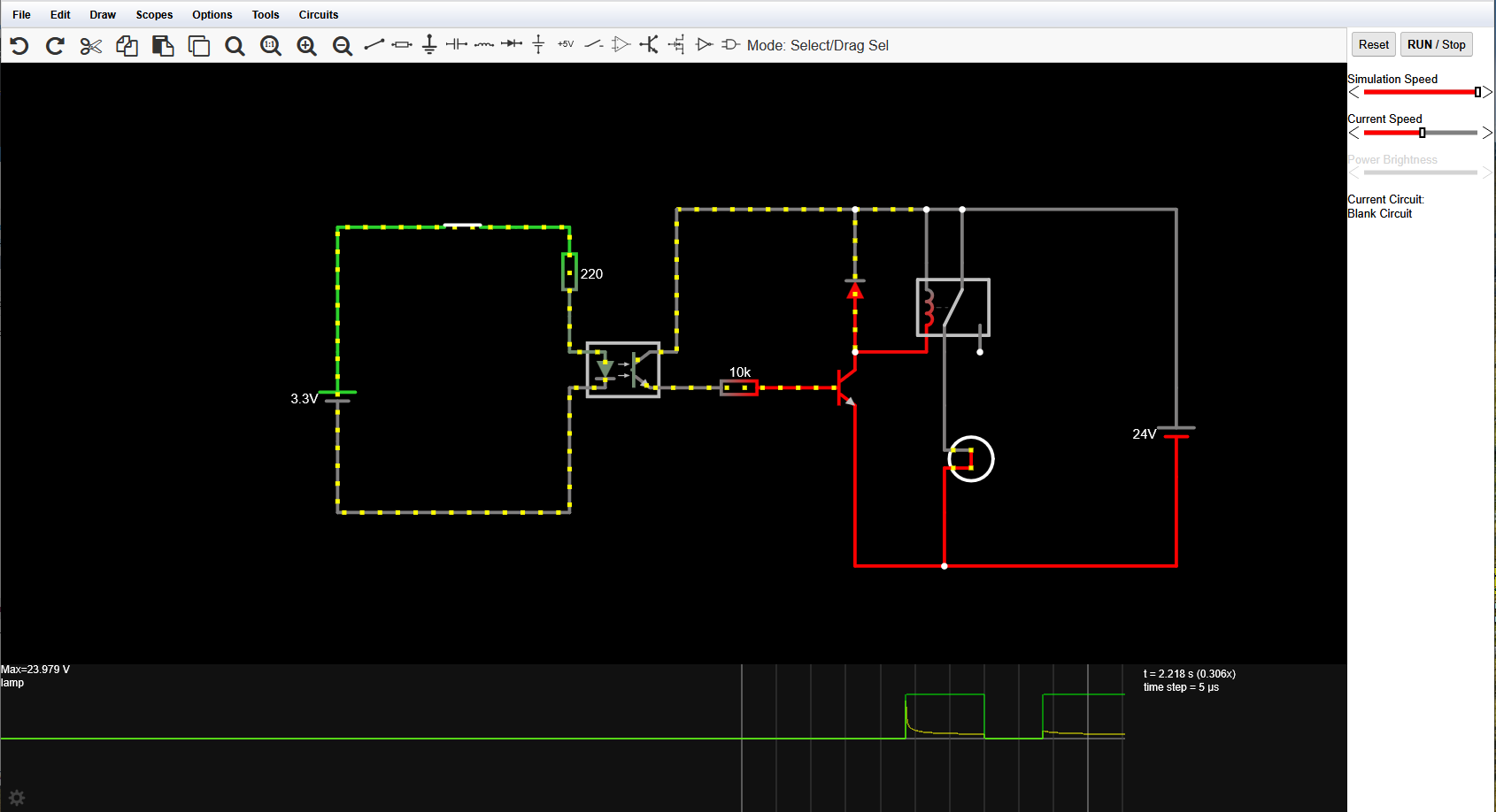
Figure 3: The circuit simulation.
Falstad Import/Export Source Code
To preserve your layout design without rebuilding it from zero, navigate to File > Export As Text, use Copy to Clipboard, and save your setup inside a local text editor note file. You can import the circuit layout immediately by pasting your saved setup string back into the software block.
<cir f="1" ts="0.000005" ic="382.76258214399064" cb="51" pb="50" vr="5" mts="5e-11">
  <Optocoupler x="512 320 512 400" f="1">
    <t vbe="0.497201677593057" vbc="0.6174787016839339" ix="2"/>
  </Optocoupler>
  <r x="512 208 512 288" f="0" r="1000"/>
  <v x="304 400 304 320" f="16" wf="0" maxv="5"/>
  <s x="368 208 464 208" f="0"/>
  <w x="464 208 512 208" f="0"/>
  <w x="304 320 304 208" f="0"/>
  <w x="368 208 304 208" f="0"/>
  <w x="512 288 512 320" f="0"/>
  <w x="512 352 512 464" f="0"/>
  <w x="512 464 304 464" f="0"/>
  <w x="304 464 304 400" f="0"/>
  <rl x="864 240 864 320" f="22" po="1" in="0.2" ron="0.05" roff="1000000" on="0.02" coR="20" of="0.015" sw="0.005" i="0.23143325769651255" ip="1"/>
  <w x="1056 512 1056 432" f="0"/>
  <w x="1056 352 1056 192" f="0"/>
  <v x="1056 432 1056 352" f="16" wf="0" maxv="24"/>
  <Lamp x="848 368 848 464" f="0" te="548.7536214190272" np="100" nv="120" wa="0.4" co="0.4"/>
  <w x="848 464 848 512" f="0"/>
  <w x="848 512 1056 512" f="0"/>
  <w x="848 320 848 368" f="0"/>
  <w x="864 240 864 192" f="0"/>
  <w x="864 192 1056 192" f="0"/>
  <w x="832 320 768 320" f="0"/>
  <w x="768 320 768 336" f="0"/>
  <w x="832 240 832 192" f="0"/>
  <w x="832 192 864 192" f="0"/>
  <w x="768 368 768 512" f="0"/>
  <w x="768 512 848 512" f="0"/>
  <d x="768 304 768 224" f="0" mo="default"/>
  <w x="768 320 768 304" f="0"/>
  <w x="768 224 768 192" f="0"/>
  <w x="832 192 768 192" f="0"/>
  <t x="720 352 768 352" f="0" pn="1" be="100" mo="default" vbe="-18.634954592949047" vbc="0.736380253837023"/>
  <r x="608 352 720 352" f="0" r="10000"/>
  <w x="768 192 608 192" f="0"/>
  <w x="608 192 608 320" f="0"/>
  <o en="15" sp="1024" f="x3" p="0">
    <p v="0" sc="40"/>
    <p v="3" sc="6.4"/>
  </o>
</cir>
Engineering Advice: Switching DC vs. AC Field Loads
While the simulation focuses on a 24VDC system, real-world relays are frequently used to switch alternating current (AC) machinery like 220VAC water pumps. Understanding the distinct stress elements of DC and AC loads on mechanical contacts is vital for your circuit’s operational lifespan.
1. Switching DC Loads (High Arc Risk)
Direct current maintains a continuous voltage level without ever dropping to a zero baseline. When physical relay contacts separate under heavy DC load conditions, a continuous electric spark (arc) forms across the widening physical gap. This high-temperature arc slowly melts, pits, and degrades the contacts over time.
- Safety Rating: A relay rated to switch 10A at 250VAC can typically only handle 10A up to 30VDC before arc degradation risks lock the contacts permanently shut.
- Suppression Fix: Always use a flyback diode (like a 1N4007) across inductive DC loads to clamp high-voltage spikes, or deploy an RC Snubber circuit across the contacts.
2. Switching AC Loads (Zero-Crossing Advantage)
Alternating current oscillates back and forth continuously, dropping down to pass through 0V exactly twice during every complete frequency cycle (100 or 120 times per second depending on your regional grid). This continuous zero-crossing behavior naturally extinguishes forming contact arc points quickly.
- Safety Rating: Relays can comfortably manage significantly higher voltage potentials (250VAC+) without premature contact erosion.
- Suppression Fix: Inductive AC field devices (motors, transformers) throw highly destructive phase-shifted noise vectors. Always wire a dedicated Metal Oxide Varistor (MOV) or AC-rated RC snubber network in parallel across the switching relay contacts to protect the system.
🛠️ Ready for the Bench?
Now that you have verified the circuit and analyzed the real-time waveforms in the safety of software, the next step is to wire it up on the test bench. Check out our comprehensive step-by-step guide to build this physical ESP32 galvanic isolation circuit on a breadboard using a real 24V Finder relay and a buck converter module.
Read the next guide: Step-by-Step Physical Build & Testing Guide →